
Duration of the online course: 35 hours and 10 minutes
4.81

(26)
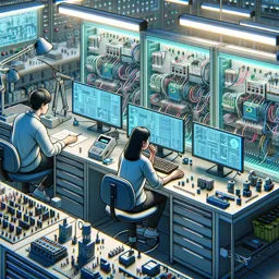
Step beyond basic electrical work and gain a clear, practical view of how modern electronics are made. This free online course connects electrical fundamentals to the real manufacturing steps that turn ultra-pure silicon into the integrated circuits inside everyday devices. If you want to understand what happens inside a fab, speak the language of technicians and engineers, or broaden your opportunities in electronics and industrial environments, this training gives you that bridge from the macro world to the nano scale.
You will develop a solid mental model of silicon as a material: why crystal structure matters, how high-purity silicon is produced, and what can go wrong when contamination enters the process. The course also helps you understand clean lab thinking and process discipline, reinforcing why particle control, water purity, and careful handling practices are essential to yield and reliability. This knowledge is valuable not only for semiconductor work, but for any role where precision, safety, and controlled processes define success.
From there, you will follow how electrical properties are engineered through diffusion and ion implantation, learning how impurities are introduced and driven into silicon to create functional regions in devices. You will also see why silicon dioxide is so central to VLSI technology and how oxidation becomes a key tool for insulation and device formation. As the flow continues, you will understand how patterns are created through lithography, how thin films are added by deposition methods, and how materials are selectively removed by etching to form complete structures. Throughout, the focus is on process understanding and the reasoning behind each step, so you can interpret terminology, troubleshoot intelligently, and connect measurements to outcomes.
Designed within professional skills for electricians and technical learners, the course supports upskilling for roles that intersect with electronics manufacturing, maintenance, QA, or high-tech facilities. By the end, you should feel confident reading process discussions, following a CMOS-oriented fabrication flow at a high level, and explaining how key fabrication choices influence device behavior and reliability.
35 hours and 10 minutes of online video course
Digital certificate of course completion (Free)
Exercises to train your knowledge
100% free, from content to certificate
Ready to get started?Download the app and get started today.
Install the app now
to access the courseOver 5,000 free courses
Programming, English, Digital Marketing and much more! Learn whatever you want, for free.
Study plan with AI
Our app's Artificial Intelligence can create a study schedule for the course you choose.
From zero to professional success
Improve your resume with our free Certificate and then use our Artificial Intelligence to find your dream job.
You can also use the QR Code or the links below.


Free CourseSiemens PLC Training
5
(10)

9h42m

32 exercises
Free CourseInstall Your Own Solar Power System
5
(1)
59m
6 exercises
Free CourseElectronic Circuits Course
5
(6)
43h25m
49 exercises

Free CourseWind Turbines
5
(3)
3h49m
19 exercises

Free CourseEngineering Circuits Analysis
5
(6)
3h11m
20 exercises

Free CourseElectronics - Nanoelectronics: Devices and Materials
4.84
(43)
40h15m
31 exercises

Free CourseElectrical engineering
4.83
(23)
11h53m
20 exercises

Free CourseBasic electronics
4.82
(22)
6h04m
30 exercises

Free CourseBeginner Electronics
4.79
(84)
5h27m
24 exercises

Free CourseElectricity course
4.78
(54)
31h41m
6 exercises
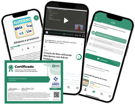
Thousands of online courses in video, ebooks and audiobooks.
To test your knowledge during online courses
Generated directly from your cell phone's photo gallery and sent to your email
Download our app via QR Code or the links below::.
Carry knowledge in your pocket.
Download the Cursa app.
There are hundreds of free courses available, with a free certificate of completion that is saved in your mobile image gallery.
Download the app to access the Course Completion Certificate for Free.

+ 10 million
students
Free and Valid
Certificate
60 thousand free
exercises
4.8/5 rating in
app stores
Free courses in
video and ebooks

Course comments: Electrical - Fabrication of Silicon
anwar haizal
It really good course for me as chemical engineer to adapt to the semiconductor manufacturing